Introduction to Verilog
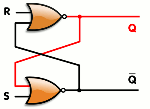
[source: http://en.wikipedia.org/wiki/File:R-S_mk2.gif]

Hardware
Description
Language
We use Verilog to describe hardware
(Other languages exist, like VHDL; no serious designer uses schematic entry)
Wires connect logic elements, have no memory, and their value is determined by what's driving them.

Elementary single bit memory unit
(Latches are considered harmful)
Elementary logic unit
"Large" memory blocks

[source: http://generatormeme.com/meme/atdmab#.UWHJ1cqbXAU]
That there is no main()?!
Everything runs concurrently
Think left to right, not top to bottom
`define ROUNDS 4 // global constants
parameter param1=<value>; // local parameters
reg  [nn:mm] foo, bar;
wire [nn:mm] oof, rab;
Creating a module:
module <module_name> (
  input  [nn:mm] <port_name_1>,
  output [nn,mm] <port_name_2>
  ...
);

  ...

endmodule
or
module (<port_name_1>, <port_name_2> ...);

  input  [nn:mm] <port_name_1>;
  output [nn,mm] <port_name_2>;

  ...

endmodule
<module_name> <unique_instance_name> (.<port_name_1>(<wire_name_1>),
                                      .<port_name_2>(<wire_name_2>));
b = a;
c = b;
r = `ROUNDS;
b <= a;
c <= b;
Always use non-blocking assignments! (unless it's in a testbench)
Think in bits!
In an FPGA every memory bit is either at a state of 0 or 1
Values can be expressed in several ways:
a = 10;
b = 4'b1010;
c = 4'd10;
d = 4'hA;
e = {2'b10, 2'b10};
f = {1'b1, 1'b0, 1'b1, 1'b0};
all represent the same bit sequence.
In simulation you'll get a value of X ('undetermined') if no initial value has been set. Again, in the FPGA it will be either a 0 or 1.
FPGA code is almost always synchronous, which means that events only happen on clock edges.
Always think about the clock; nothing happens without it
Since everything runs all the time, we use 'states' to determine when to evaluate an input signal and when to change an output. All but the very basic HDL code has 'finite state machines' that control the behaviour of the design.

[source: http://en.wikipedia.org/wiki/File:Turnstile_state_machine_colored.svg]
module turnstile (
  input CLOCK,
  input PUSH,
  input COIN,
  output UNLOCKED
);

reg state

assign UNLOCKED = state;

parameter LOCKED_STATE=1'b0, UNLOCKED_STATE = 1'b1;

always @(posedge CLOCK) begin
  if (reset) state <= next_state;
  else state <= LOCKED;
end

always @(posedge CLOCK) begin
  if (reset) next_state <= LOCKED_STATE;
  else
    case (state)

      LOCKED_STATE:
      begin
        if (coin == 1'b1)
          next_state <= UNLOCKED;
      end

      UNLOCKED_STATE:
      begin
        if (push == 1'b1)
           next_state <= LOCKED;
      end

      default:
      begin
        // ALWAYS have a default for a case statement,
        // even if all possible cases are covered
        next_state <= LOCKED;
      end
  endcase
end
* this snippet is a good start, but more is needed for a robust design
Finite state machines can have many, quite complicated, states, so it's good practice to draw a state diagram on paper before starting to code! A concise intro to FSMs in Verilog is here.
Ask yourself
- Is it working in simulation?
- Is the clock working and reaching the logic?
- Is my logic still there?
Don't freak out if you get a gazillion warnings; it's perfectly normal in this world of FPGA tools!
Other than searching for the error message, http://electronics.stackexchange.com or http://stackoverflow.com are good places to find and ask questions.
Create a lower frequency clock from the main 50 MHz clock and output a pattern on the LEDs
Create a single pulse of a particular clock period from an incoming pushbutton signal
Edge detect circuit:

Do one or both of the following
Output a Fibonacci number update on the LEDs (in binary) whenever KEY1 is pressed. Reset the pattern when KEY0 is pressed. When the Fibonacci number exceeds what can be displayed on the LEDs, display a unique pattern (such as blinking all LEDs multiple times) on the LEDs, then reset.
Example state diagram (can be done differently and more efficiently):

Using the switches, LEDs and pushbuttons, implement a 4-bit 4-gidit lock. Each combination digit is entered using the switches and a press of KEY1. A pattern should let the user know whether the combination succeeded or failed. (Watch out for insecure implementations!) Extra credit for locking the interface after three wrong attempts. Super extra credit for allowing the user to re-set the initial combination after a successful entry.
Hints:
- Start by connecting each switch to an LED and see if it turns on/off when the switch is moved positions
- Create a state diagram on paper before starting to coding
- An example design can be found in the repo; use it if you're stuck, or as a starting point
Create a 4-bit arithmetic logic unit (ALU) using the LEDs, pushbutton and switches. The ALU should support addition, subtraction, multiplication, and division of 4-bit numbers. Use the switches and pushbuttons as for digit and arithmetic operation choice. Use the LEDs for displaying status and results.
Choose a DE0-nano peripheral of your choice and write a driver for it. UART may be simplest (implement transmit first), though implementing basic I2C and SPI functionality is also doable. Be creative!