This is a simple 3-stage RISC-V CPU with Cache implementation, which is capable of processing all types of RISC-V instructions. Data hazards, control hazards are all taken care of, and the CPU will not wait when branching.
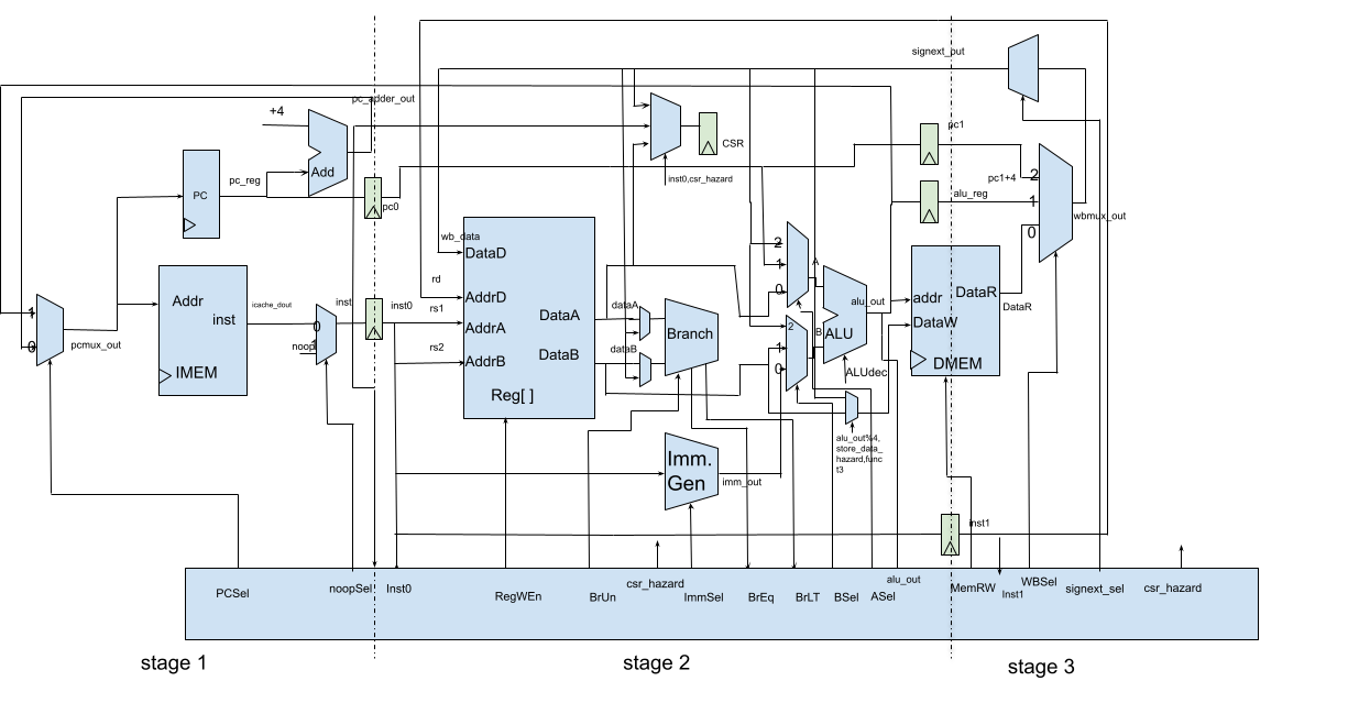 The pipeline diagram is shown above
- Submodules explanation:
- ALU: consist of two modules: ALU and ALU decoder. ALU decoder input the instrucƟon and decode into ALU operaƟons. ALU input ALU decode result and two input data and conduct computaƟon.
- Branch_compare: input two data and BrUn signal, determine if BrLT and BrEq is true and output back to the control module.
- Immediate generator: input imm select signal from control and use combinaƟonal logic to determine what kind of immediate to generate, output generated immediate number.
- Signext: input data, signext_sel, memory address, and 3 bits funcƟon code. Use signext_sel to determine data length dealing, like lw,lh,lb. And use memory address%4 to determine which part of data is being loaded, then do sign extension.
- Control: input instrucƟon from different stages, BrLT, BrEq, reset, alu_out data.
- Control signal:
- i)PC_sel: control pc_mux to select from alu_out(Branch, jump) or pc_adder_out(other)
- ii)RegWEn: register file write enable, enabled in instrucƟons need write back
- iii) BrUn: if instrucƟon is unsigned, then this signal should be high
- iv) noopSel: if BrLT|BrEq is true, then noopSel is 1Peter Peng & Christopher Keesey Fall 2021 ASIC Lab
- v)Signext_Sel: if the instrucƟon is load half word, then it is 1, if the instrucƟon is load byte, then it’s 2. Otherwise it’s 0, no sign extension.
- vi) ASel,BSel: determine whether to take data from regfile or immediate generator or pc or signext_out(ALU forward). Method of hazard detecƟon: if the current instrucƟon need data from the regfile and the former instrucƟon needs write back whose rd is neither 0 or equal to one of rs of the current instrucƟon or equals to both, then there’s a hazard
- vii) ImmSel: determine what type of immediate number needs to be generated in the current instrucƟon.Determined by instrucƟon in stage 2
- viii) WBSel: determine whether to write back pc value or ALU value or memory data to the regfile. Determined by instrucƟon in stage 3
- ix) MemRW: determined by the instrucƟon(sw,sh,sb) and memory address(addr%4), it can be output to memory to write different parts of the word.
- x)Store_data_hazard: hazard control for store instrucƟons.
- xi) Branch_hazard: hazard control for branch instrucƟons.
- xii) Csr_hazard: hazard control for csr instrucƟons.
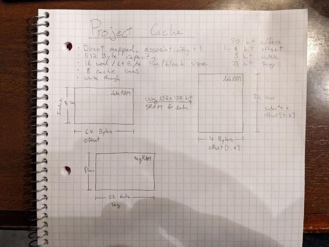
- The 512 Byte cache consisted of two SRAMs and was constructed using a
FSM. We implemented a direct mapped cache with 8 64 Byte blocks and a
write-through policy. This corresponded to spliƫng the 30-bit requested memory
address into a 4-bit offset, 3-bit index, and 23-bit tag. A 64x32 bit SRAM was used to
store the tags of data stored in the cache with the least significant bits of the 32-bit
lines used. The data was stored in a 256x128 bit SRAM because it had a byte mask
input. To sƟll have 64 Byte logical blocks, 4 lines of this SRAM were used per cache
block. The valid bit for each tag line was originally kept in tagRAM as the MSB, but
this gave us problems due to it being uniniƟalized to 0. Instead, we created an 8 bit
register to keep track of the valid bit for each cache block.
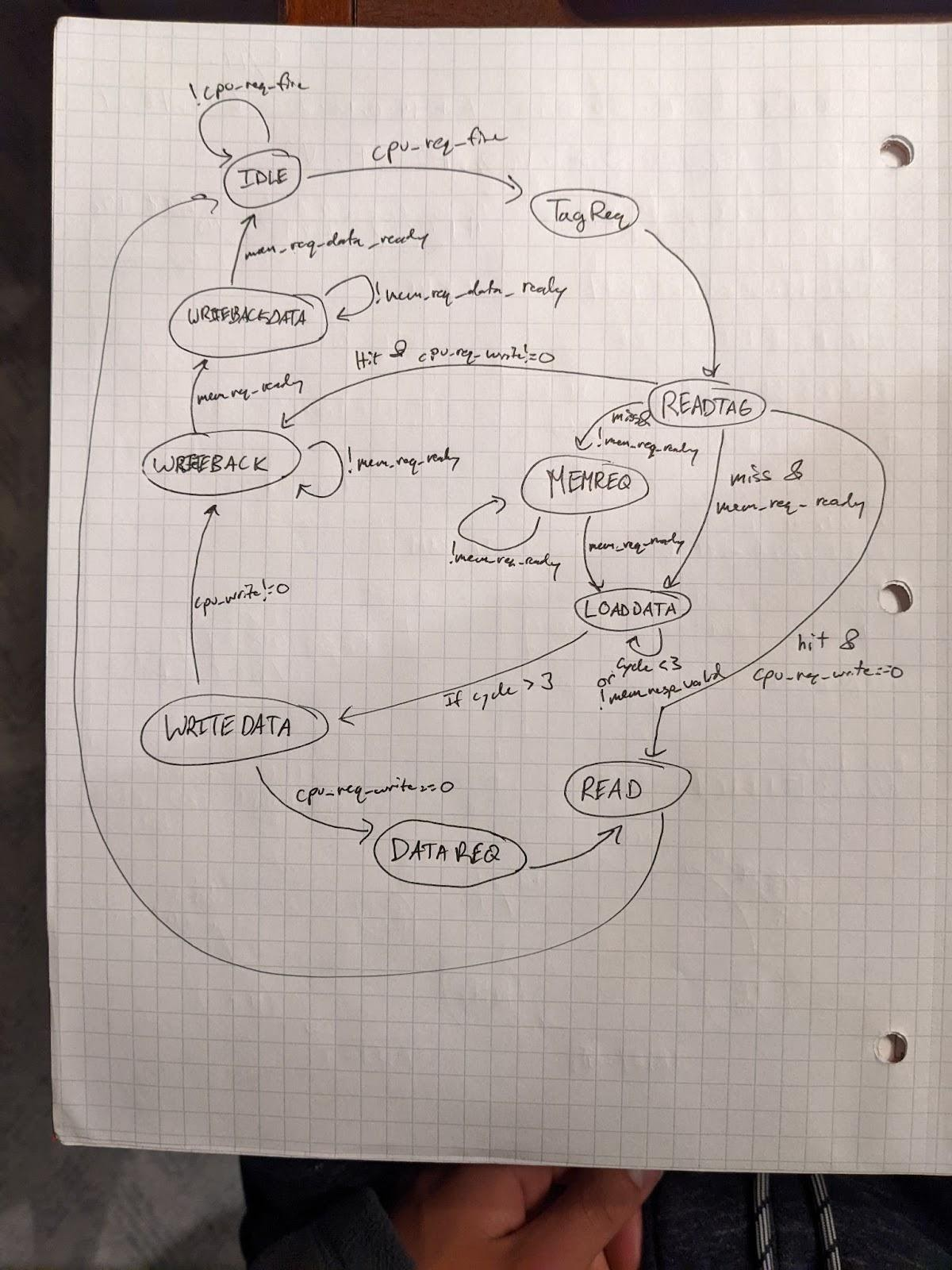
- The FSM consisted of 10 states, not all of which were used in each type of transacƟon. Here
are the states and their funcƟonality:
- IDLE: send ready signal to cpu, set response to invalid and wait unƟl a valid request is sent from the cpu.
- TAGREQ: wait for the tagRAM to output valid tag data for the requested address
- READTAG: If tag is invalid or is not at the index requested, cache miss. On cache miss, make a request to main memory. If there is a cache hit, i.e. the tag matches that stored in the cache at the requested index, read from dataRAM. If write, set inputs to dataRAM and move to writeback.
- MEMREQ: wait for memory to be ready to receive a request.
- LOADDATA: Load memory response into dataRAM over 4 cycles.
- WRITEDATA: If memory write, write data to dataRAM.
- DATAREQ: Request data from dataRAM at proper offset.
- READ: Set cpu response to proper data.
- WRITEBACK: make a main memory request.
- WRITEBACKDATA: write through data to main memory.
- The paths of each type of transaction are as follows:
- Memory Read, cache miss: IDLE→TAGREQ→READTAG→MEMREQ (if memory is not ready)→LOADDATA (x4)→WRITEDATA→DATAREQ→READ→IDLE
- If memory is ready immediately, 11 cycles
- Memory Read, cache hit: IDLE→TAGREQ→READTAG→READ→IDLE
- 4 cycles
- Memory Write, cache miss: IDLE→TAGREQ→READTAG→MEMREQ→LOADDATA(x4)→WRITEDATA→WRITEBACK →WRITEBACKDATA→IDLE
- If memory is ready immediately, 11 cycles
- Memory Write, cache hit: IDLE→TAGREQ→READTAG→WRITEBACK→WRITEBACKDATA→IDLE
- 5 cycles
- Note: Cache does not wait for memory to finish wriƟng back before returning to IDLE state.
The MEMREQ stge ensures that memory is ready before the next transaction